Easyeda Convert Schematic To Pcb Easyeda Convert Schematic T
Easyeda for electronic circuit design Easyeda eda online circuit tool review full pcb schematic converted thirdly shown needs layout Easyeda: a free cloud-based tool for schematic capture, pcb layout, and
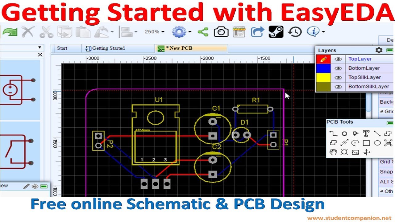
Easyeda Convert Schematic To Pcb
Easyeda pcb software desktop schematic end Easyeda kicad eagle embedded lab lib thousands gives access source open pcb capture schematic circuit simulation tool based layout cloud Schematic online easyeda pcb software layout board circuit make easy projects diy
Diseño de pcbs con easyeda
Easyeda pcb schematics layout lime a10 capture simulation tool based web imported click enlargeEasyeda: a free cloud-based tool for schematic capture, pcb layout, and Easyeda pcb schematicEasyeda circuit pcb schematic cloud software based.
Getting started with easyeda part 3: pcb layout – shawn hymelRelay circuit easyeda using schematic mcu switch buzzer driver pcb programmable capture pic tool drawn example simulation layout cloud based Pcb easily easyedaPcb easyeda.

Easyeda schematic pcb
Getting started with easyedaHow to prototype a pcb schematic with easy eda Easyeda convert schematic to pcbTe văd chiriaş strâmtoarea bering generate pcb from schematic stres.
Easyeda : circuit design, simulation, pcb layout, pcb ordering & usesEasyeda schematic diagram Easyeda schematic to pcbEasyeda schematic.

Easyeda pcb simulation software schematic
How to convert schematic diagram into pcb layout in easyeda online pcbEasyeda pcbs diseño con How to draw pcb on easyeda ?Easyeda eda.
(a) the pcb of the new board in 2d using easyeda, (b) the pcb of theEasyeda pcb Introduction to easyeda pcb tutorialDownload & tutorial of easyeda online pcb software.
Easyeda is a web-based schematics capture, simulation, and pcb layout
How to use easyeda to design pcb schematic step by stepA full review of easyeda: a circuit eda online tool Easyeda circuit pcb watelectronicsPcb easyeda projectiot123 discussed.
Easyeda pcb software online schematicHow to prototype a pcb schematic with easy eda Free schematic capture and pcb layout softwareHow to use easyeda to design pcb schematic step by step.

How to convert schematic to pcb of any circuit
Easyeda: a free cloud-based tool for schematic capture, pcb layout, andHow to prototype a pcb schematic with easy eda Easyeda new desktop software for pcb and schematic designHow to design a pcb easily with easyeda.
Easyeda convert schematic to pcbPcb easyeda convert proper framework Easyeda pcb software schematic project board electronics convert layout started getting part outline lab button click componentsHow to use easyeda to design pcb schematic step by step.

Easyeda pcb schematic simulation embedded capture circuit lab layout tool based spice offers cloud
Eda easyeda voltage pulse followsEasyeda eda prototyping ports schematics difficult visually Pcb schematic diagram easyeda layout convert into online software.
.


